 Custom Quartz Infrared Heaters
Custom Quartz Rings
| Parameter | Typical Range |
|---|---|
| OD | 10–300 mm |
| ID | 5–280 mm |
| Thickness / height | 2–20 mm |
| Flatness | ≤0.02 mm over 100 mm |
| Parallelism | ≤0.05 mm |
| Concentricity (ID-to-OD) | ≤0.02–0.05 mm |
| Surface finish | Ground standard; polished on request |
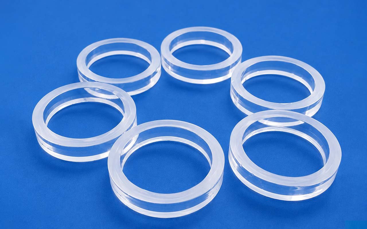
Precision quartz rings machined to OD, ID, flatness, and parallelism — built around whatever hole, groove, or step your equipment interface needs.
OD, ID, thickness, and any groove or hole feature are coupled — a feature cut close to the ID or OD affects flatness and remaining wall around it. Send the full feature layout, not the ring outline alone.
Precision Quartz Rings for Semiconductor, Vacuum and Thermal Equipment
Rings are used as spacers, retainers, mounting collars, and sealing surfaces across semiconductor, vacuum, and thermal equipment. Plain (no features), stepped (a shoulder or lip machined in), grooved (for an O-ring or retaining feature), and drilled (mounting or process holes) configurations are all made from the same OD/ID/thickness starting point.
Ring OD, ID, Thickness, Flatness and Parallelism
Flatness and parallelism are checked per face — a ring can be flat on each face individually and still have the two faces out of parallel, which matters wherever the ring seats against another part or seals a joint. Concentricity between ID and OD matters most where the ring centers a shaft, tube, or another component through its bore.
Grooves, holes, and steps are added by CNC grinding or mechanical/diamond drilling (down to about Ø0.8 mm at ±0.02 mm); tell us feature position relative to ID or OD so the whole cross-section can be checked in one measurement. Before shipment we check OD, ID, thickness, flatness, parallelism, concentricity, and feature dimensions.
ID × OD × TQuote Dimensions
±0.1 mmSize Reference
FlatnessFace Control
ParallelismStack Control
JGS2Material Option
Low OHMaterial Option
Annular Geometry
ID, OD and Face Thickness Must Share the Same Datum System
| Controlled Feature | Reference Capability / Requirement |
|---|---|
| ID × OD × Thickness | All three finished dimensions stated together |
| Dimensional Tolerance | ±0.1 mm industry-reference level; tighter critical features quoted by geometry |
| Flatness | Applied to functional seating faces |
| Parallelism | Controls axial stack-up between the two faces |
| Concentricity | ID referenced to OD where radial fit matters |
| Edge | Chamfer, radius or fire-polished edge by function |
| Secondary Features | Steps, grooves, holes or slots dimensioned from the seating face |
| Material | JGS2-class or low-OH quartz according to equipment use |
Ring Configuration
Separate Seating Faces from Non-Critical Edges
| Form | Controlled Features | Use |
|---|---|---|
| Plain ring | ID, OD, thickness and faces | Spacer or isolation ring |
| Stepped ring | Two diameters and shoulder height | Located equipment interface |
| Grooved ring | Groove width, depth and radius | Seal or retaining feature |
| Drilled ring | Hole count, diameter and PCD | Mounted or indexed component |
Available Forms
Configurations Defined by the Process
Plain RingSimple annular spacer with controlled faces
Stepped RingShoulder or counterbore for radial location
Grooved RingSeal, retaining or flow groove by drawing
Drilled RingBolt or alignment holes located from a defined PCD
Applications
Sealing, Spacing and Equipment Isolation
Semiconductor EquipmentLow-OH quartz rings for process assemblies
Vacuum HardwareRigid annular seating and isolation components
Thermal EquipmentQuartz spacers around high-temperature zones
Custom FixturesStepped or drilled rings matched to mating parts
Product Examples
Product Forms and Finished Components
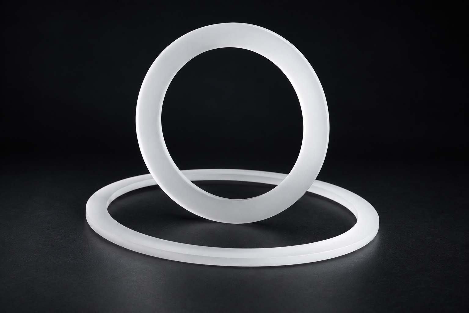
Need a precision quartz ring?Send ID, OD, thickness, critical faces, concentricity, chamfers and every groove or hole dimension.
Open the Product ConfiguratorEngineering Data
Grade-Qualified Material Purity
Electric-fused / flame-fused quartz: SiO₂ ≥99.99%; synthetic JGS1-grade fused silica: ≥99.999%. Grade and lot certificate govern supplied material.
Customize This Product
Enter your dimensions of Custom Quartz Rings — the technical drawing updates instantly, then request a quotation.
Technical Drawing
Drawing redraws live · blue hatched area = cut section · all dimensions in mm
Parameters
Every field is editable — drawing, weight estimate and part code update instantly.
Common Options
pcs
Configuration Summary
Attached to your inquiry automatically when you press “Use This Configuration”.
—