 Custom Frosted & Printed Quartz Plates
Custom Quartz Substrates
| Parameter | Factory Standard | Manufacturing Limit |
|---|---|---|
| L × W | Up to 200 × 200 mm | Larger on request |
| Thickness | 0.1–5 mm | Thinner on request |
| Flatness | ≤5 µm over typical substrate size | Tighter, confirmed per order |
| Parallelism | ≤0.02 mm | Tighter, confirmed per order |
| Surface finish | Polished standard | Ground for non-optical use |
| Feature (hole/groove) position tolerance | ±0.02–0.05 mm | Tighter, confirmed per order |
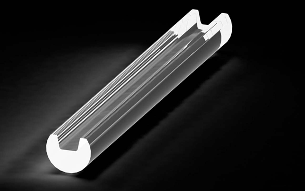
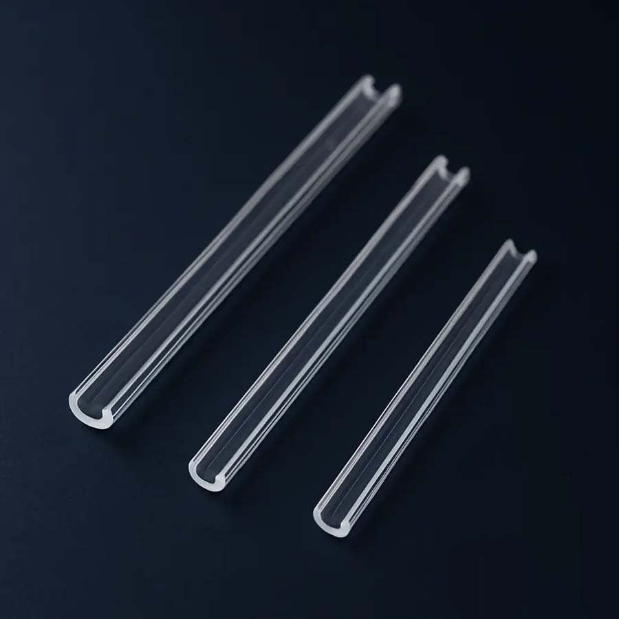
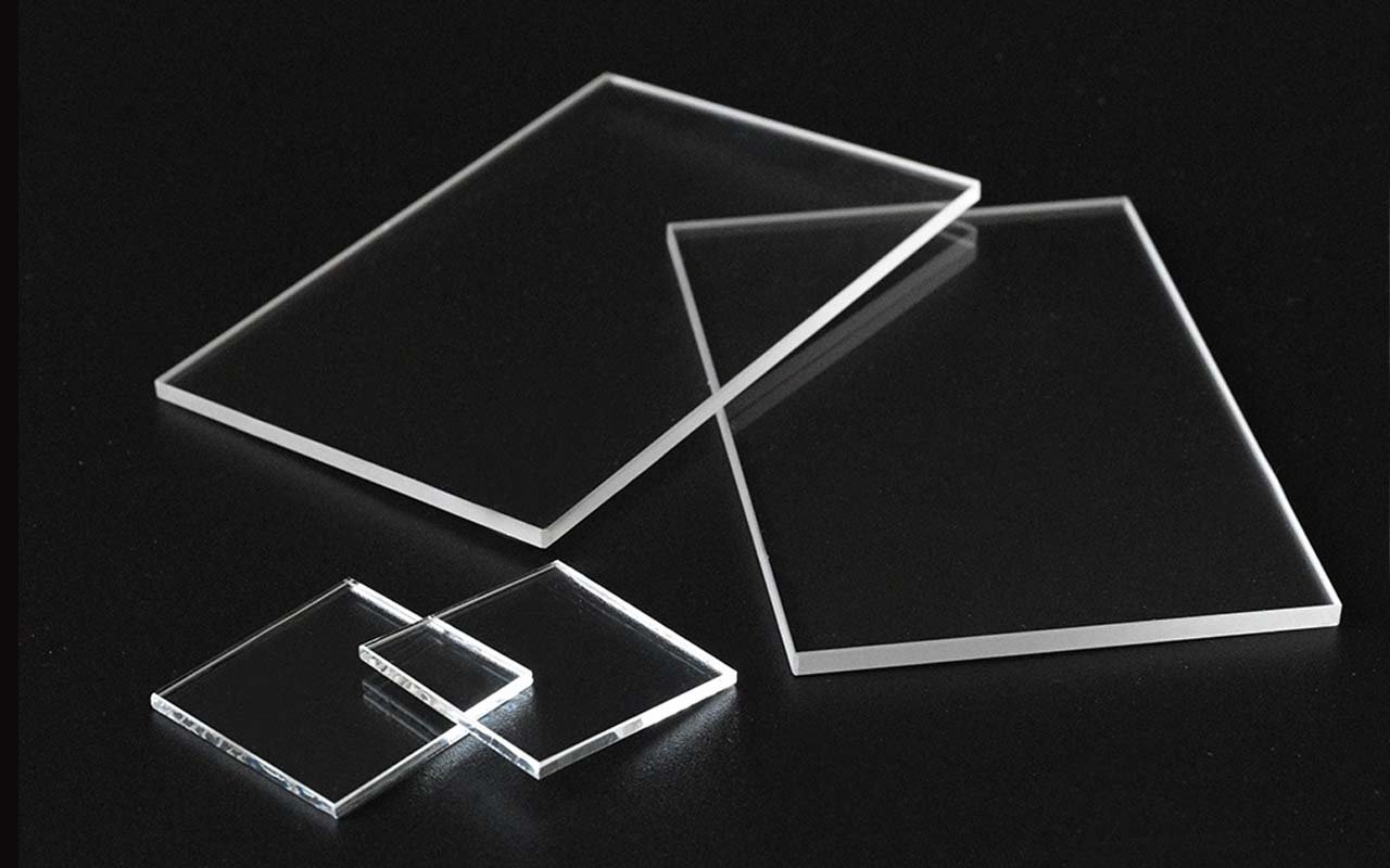
Flat quartz stock finished for optical, MEMS, and microfluidic use — where flatness, parallelism, and feature position matter more than plate size alone.
Substrates are usually thinner and flatter-spec than general plate stock, so thickness and flatness are the two numbers that most limit each other here — a thin substrate at a large L×W is the hardest combination to hold flat. Confirm both together.
Flatness, Parallelism, Surface Finish and Feature Position
Flatness and parallelism are specified independently — a substrate can be flat on each face individually and still have the two faces out of parallel with each other, which matters for anything mounted or bonded against a reference. Where holes, grooves, or alignment marks are added, their position is checked against the substrate's outer edge or a stated datum, not just against each other.
Quartz Substrates Factory Standard & Manufacturing Limit
The table above is what's repeatable without added lead time. Plain (as-cut or ground), polished, drilled, and grooved substrate configurations all start from the same flat stock — polishing, drilling, and grooving are added steps, so confirm which combination your part needs rather than assuming all features are compatible with the tightest flatness spec at once.
λ/4–λ/10Reference Surface Figure
≤1 nm RaReference Nano-Polish
JGS1UV-Grade Option
≥99.99%Natural SiO₂ · synthetic ≥99.999%
SSP / DSPSurface Configurations
Coating ReadyPrepared Working Face
Substrate Definition
The Working Surface Drives the Specification
| Controlled Feature | Reference Capability / Requirement |
|---|---|
| Material | JGS1 or synthetic fused silica selected by wavelength and contamination need |
| Length × Width | Square, rectangular, strip or drawing-specific substrate |
| Thickness | Specified with thickness tolerance and polishing allowance |
| Surface Figure | λ/4 or λ/10 industry-reference levels over the functional area |
| Surface Roughness | Reference ≤1 nm Ra for double-side nano-polished workFinal value depends on material, area and inspection method |
| Parallelism | Specified between the two working faces where bonding or optical alignment requires it |
| Feature Position | Holes, grooves and marks referenced to the same substrate datums |
| Coating Interface | Cleanliness, edge exclusion and working-face identification |
Surface Selection
Choose Only the Finish the Process Uses
| Surface Level | Controlled Result | Typical Process |
|---|---|---|
| Ground / Lapped | Thickness and flat support surface | Fixtures, carriers and further polishing |
| Single-Side Polished | One optical or coating face | Filters, sensors and instrument substrates |
| Double-Side Polished | Two functional faces with parallelism | Bonding, microfluidics and transmission |
| Nano-Polished | Reference ≤1 nm Ra working surface | High-quality coating and biochip interfaces |
Substrate Forms
Flat Bases for Optical and Microfabricated Systems
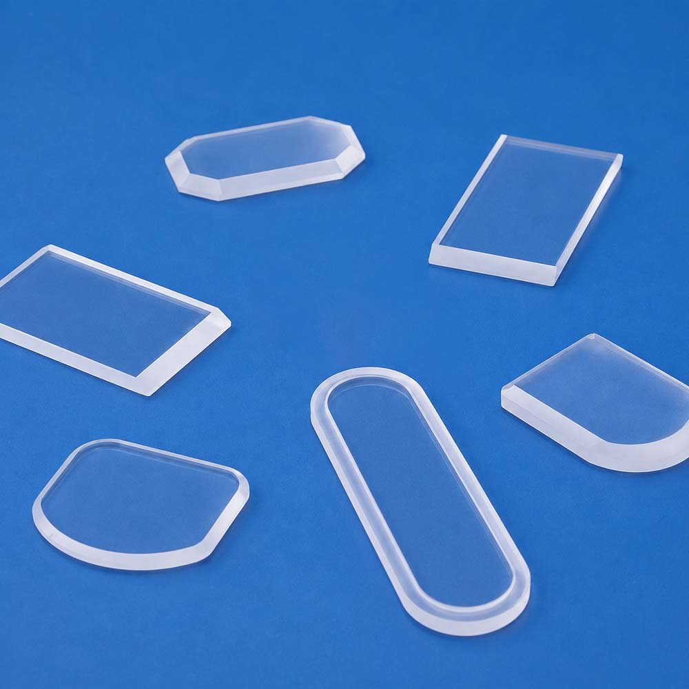
Square / RectangularGeneral polished base for coating, bonding and patterning
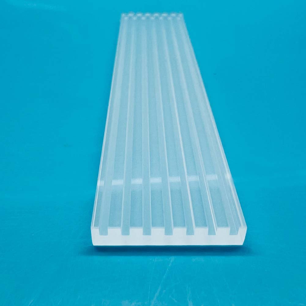
Strip SubstrateLong narrow format for filters, sensors and array devices
Featured SubstrateHoles, grooves or alignment marks tied to plate datums
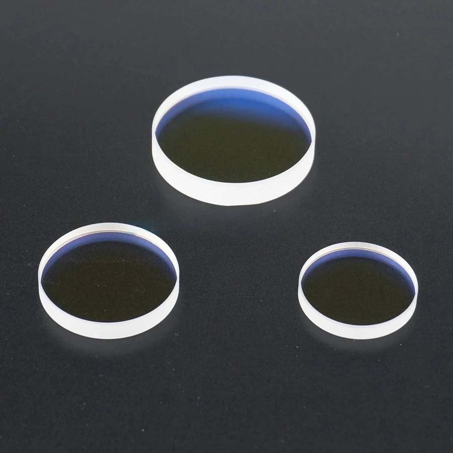
Coating-Ready SurfaceClean polished face with edge exclusion and orientation defined
Applications
Processes Built on Quartz Substrates
Optical CoatingsPolished bases for filters, mirrors and wavelength-selective layers
Biochips & SensorsLow-background transparent platforms for patterned sensing surfaces
Microfluidics & MEMSFlat quartz layers for channels, bonding and device structures
Optical FiltersControlled surface figure and parallelism for coated transmission elements
Product Examples
Product Forms and Finished Components
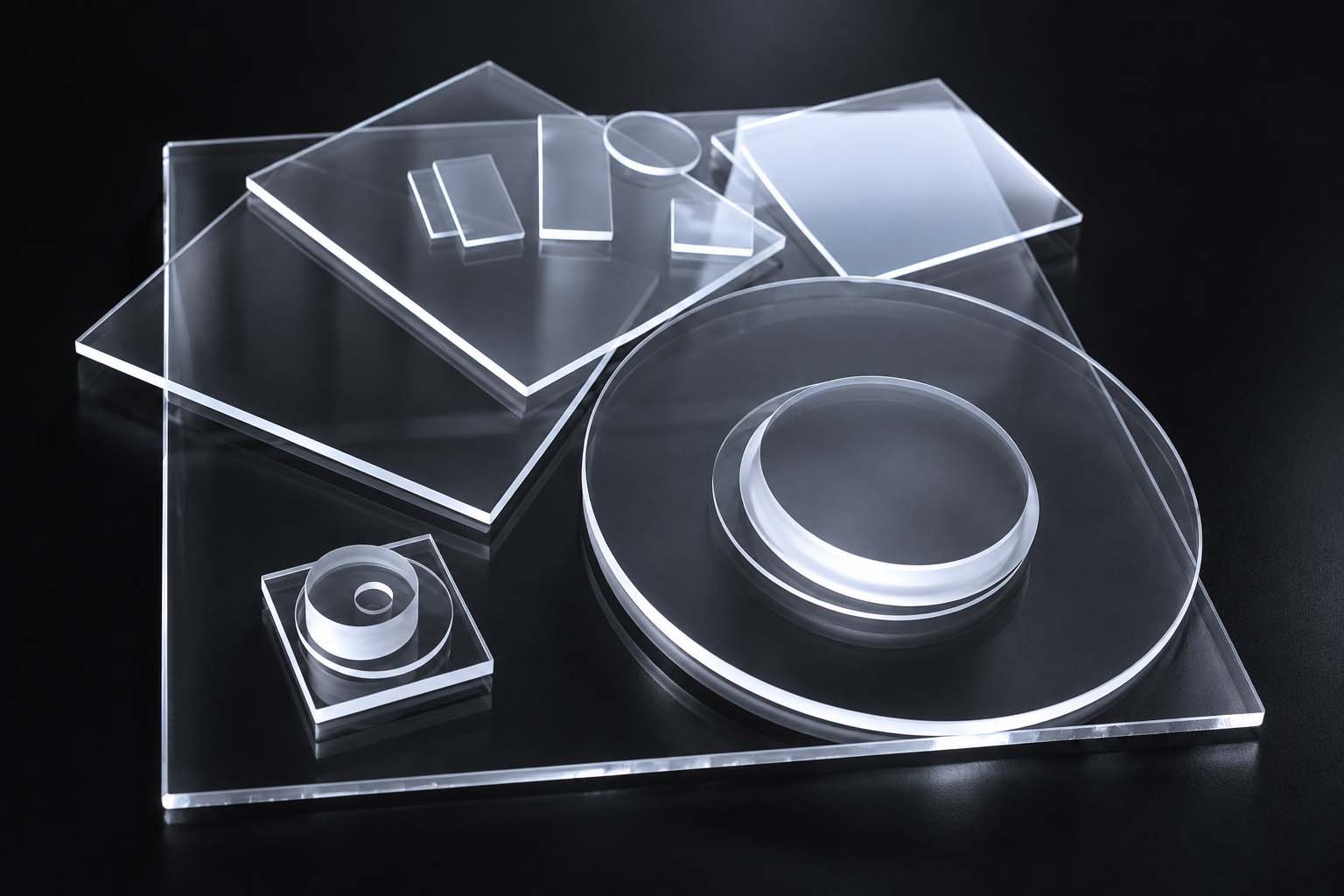
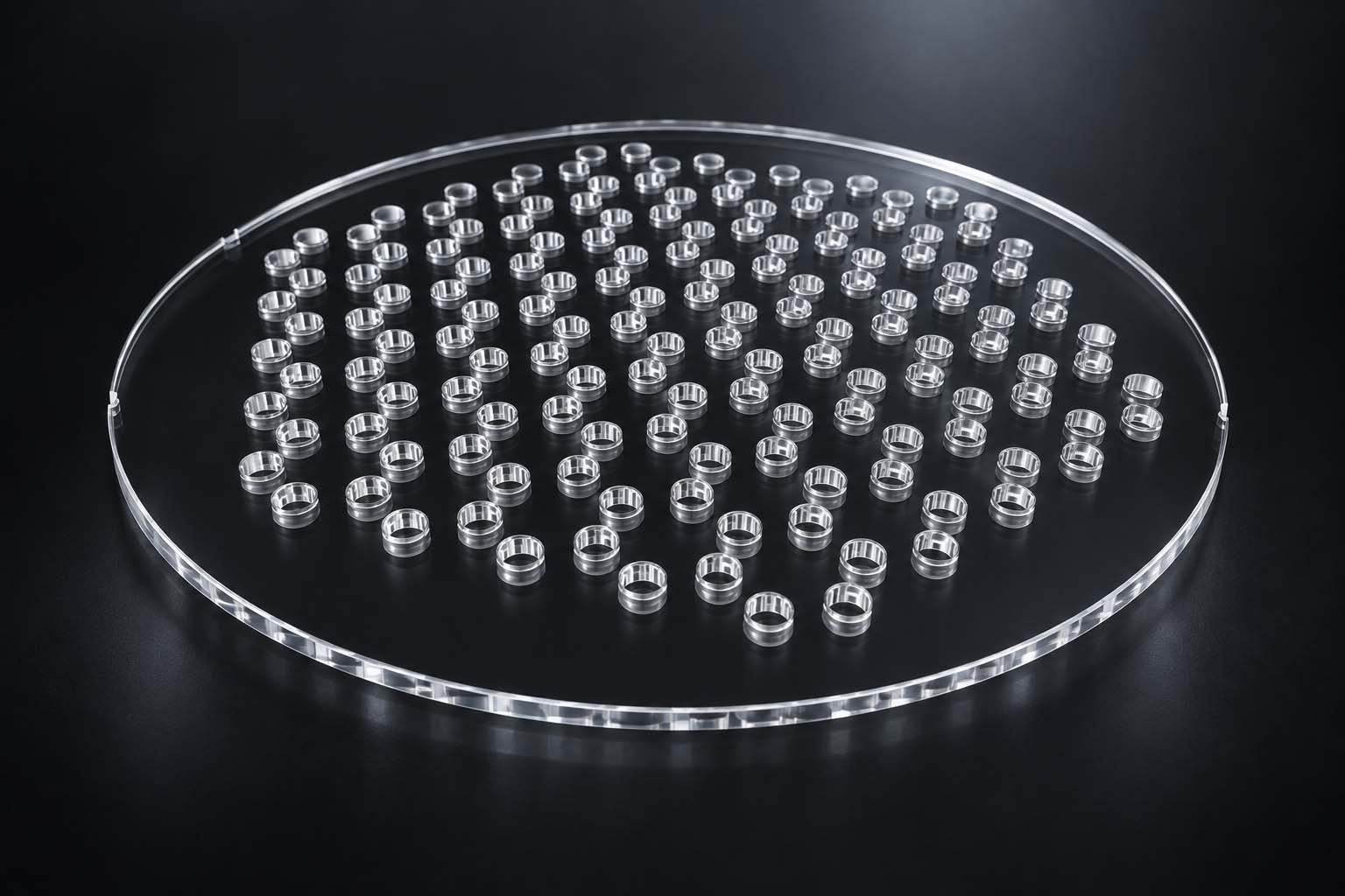
Need a substrate prepared for coating or bonding?Send size, thickness, material, surface figure, roughness, parallelism and edge-exclusion drawing.
Open the Plate ConfiguratorEngineering Data
Grade-Qualified Material Purity
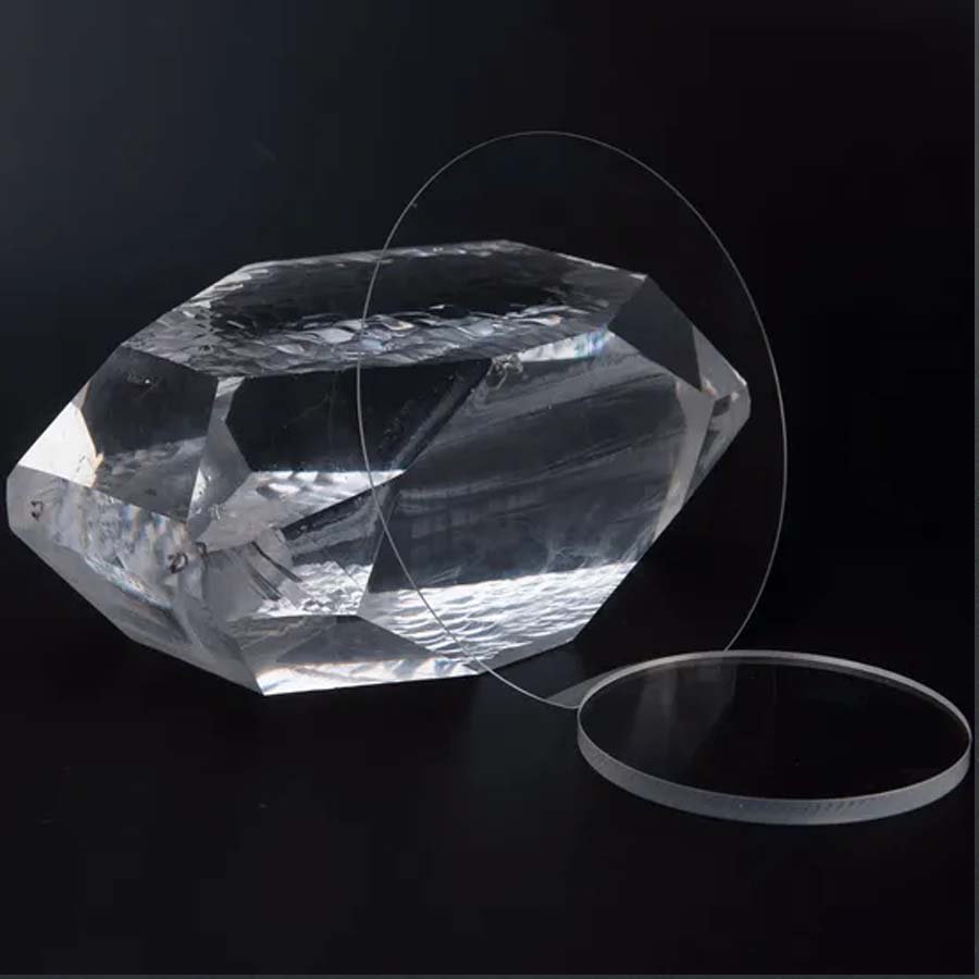
Electric-fused / flame-fused quartz: SiO₂ ≥99.99%; synthetic JGS1-grade fused silica: ≥99.999%. Grade and lot certificate govern supplied material.
Engineering Data
Surface-Figure Acceptance
For λ/10 acceptance, state the reference wavelength (633 nm unless agreed otherwise), measurement aperture and excluded edge zone, surface figure versus transmitted wavefront, peak-to-valley or RMS metric, mounting condition and interferometric test method. Ra ≤1 nm is a separate surface-roughness specification and does not substitute for figure acceptance.
Customize This Product
Enter your dimensions of Custom Quartz Substrates — the technical drawing updates instantly, then request a quotation.
Technical Drawing
Drawing redraws live · blue hatched area = cut section · all dimensions in mm
Parameters
Every field is editable — drawing, weight estimate and part code update instantly.
Common Options
pcs
Configuration Summary
Attached to your inquiry automatically when you press “Use This Configuration”.
—