 Custom Frosted & Printed Quartz Plates
Custom Quartz Wafers
| Parameter | Factory Standard | Manufacturing Limit |
|---|---|---|
| Diameter | 25.4–150 mm (1–6 in) | Non-standard sizes on request |
| Thickness | 0.2–3 mm | Thinner on request, size-dependent |
| TTV (total thickness variation) | ≤5 µm | Tighter, confirmed per order |
| Bow | ≤15 µm | Tighter, confirmed per order |
| Warp | ≤20 µm | Tighter, confirmed per order |
| Surface finish | Single-side polished (SSP) or double-side polished (DSP) | — |
| Surface roughness | Ra < 1 nm, polished | — |
| Edge | As-cut, rounded, or with orientation notch/flat | — |
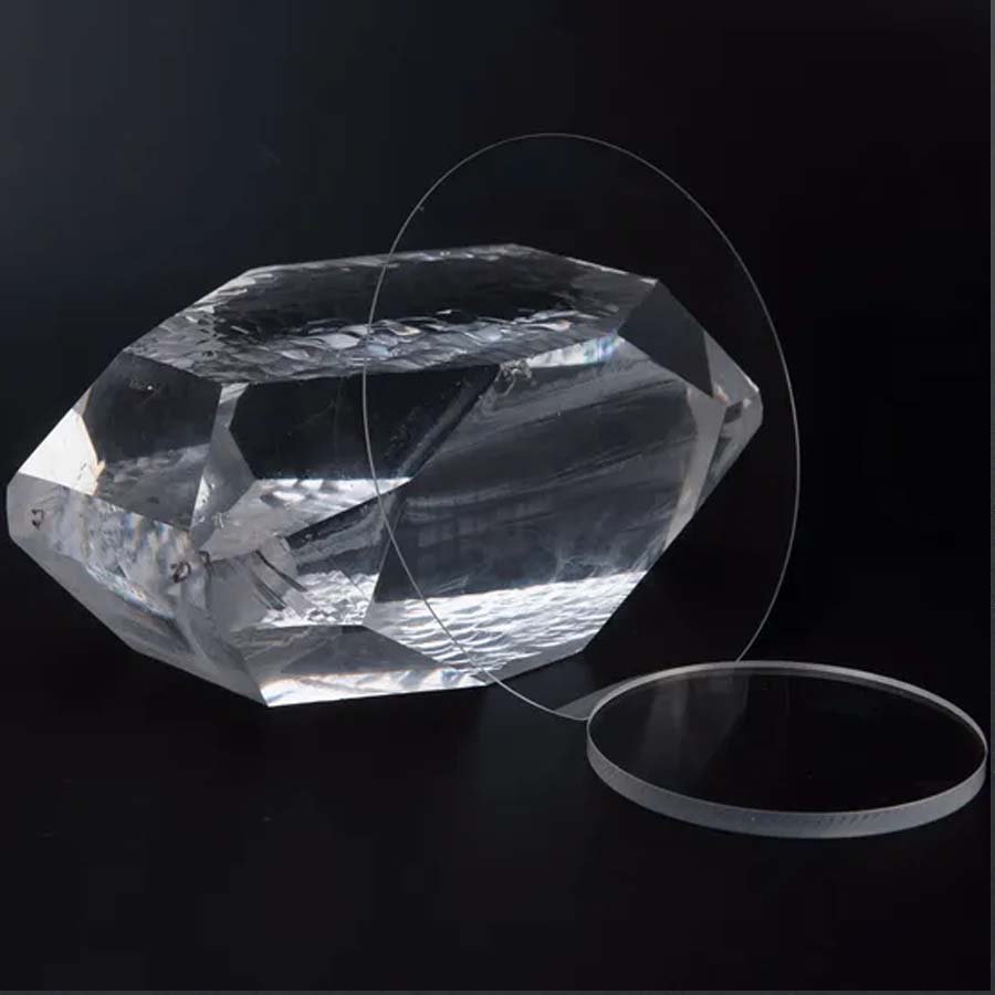
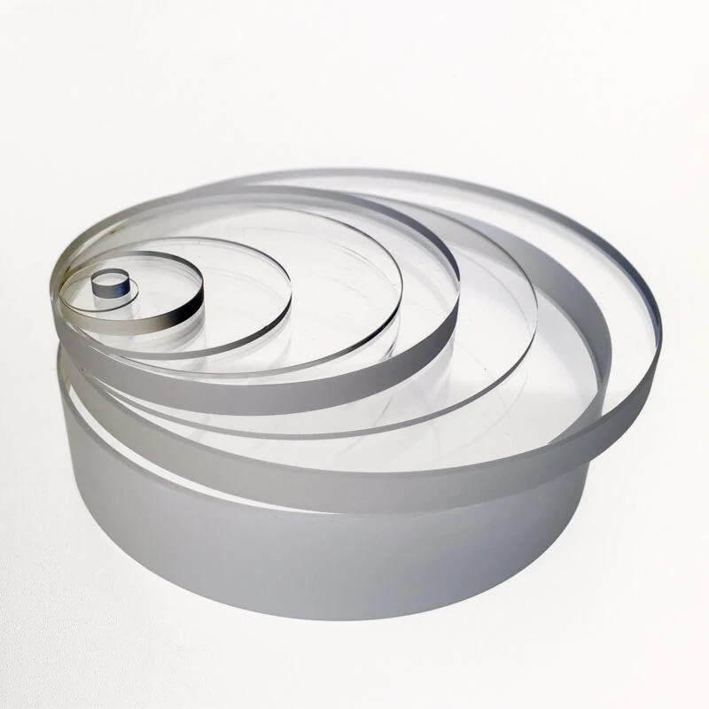
Quartz wafers for semiconductor, MEMS, and optical applications, sized and polished to the geometry your process actually needs — not just a thin round disc.
Diameter, thickness, TTV, bow, and warp are one coupled set, not separate specs — a large-diameter, thin wafer amplifies geometric instability, so tighter TTV/bow/warp gets harder to hold as diameter goes up and thickness goes down. Confirm the full combination, not one number in isolation.
Quartz Wafer Sizes, Polish Options and Edge Formats
Standard diameters follow common semiconductor wafer sizes (1", 2", 3", 4", 6"); other diameters are available but confirmed per order rather than offered as standard stock. Single-side polish is typical when only the device side needs optical-quality finish; double-side polish is used when both faces are in the optical path or need matched flatness. Edge format — as-cut, rounded (to reduce chipping in handling), or with a notch/flat for orientation — is chosen based on your process tooling, not by default.
TTV, Bow, Warp and Surface Finish
These three geometry numbers describe different things and are measured differently: TTV is the thickness variation across the wafer, bow is the deviation of the wafer's center from a reference plane with the wafer unclamped, and warp is the total peak-to-valley deviation across the surface. A wafer can meet a TTV spec and still fail a bow or warp spec — specify what your process actually depends on rather than assuming one number covers all three.
Quartz Wafers Factory Standard & Manufacturing Limit
The table above is what's repeatable without added lead time. Pushing thickness down at a large diameter is the combination most likely to need confirmation before we commit to a schedule — thin, large-diameter wafers are the hardest to hold flat through grinding and polishing.
Choosing Quartz Wafer Thickness and Surface Quality
Thickness is usually set by your process (mechanical strength needed for handling, or a target for later thinning) rather than chosen for its own sake — tell us your end-use thickness and whether it's a final spec or a starting point for further thinning on your side. Surface quality (roughness, particle/scratch requirements) should match what your process actually inspects for, since tighter-than-needed surface specs add cost without adding function.
Wafer Grinding, Thinning, Polishing and Edge Finishing
Wafers are cut from ingot or blank stock, then ground to rough thickness, thinned to final thickness, and polished on one or both sides as specified. Edge rounding or notching is done after polishing so it doesn't affect the flat surfaces. Before shipment we check diameter, thickness, TTV, bow, warp, surface condition, and edge format; particle and scratch inspection is reported where our inspection capability supports it — confirm your specific requirement so we can tell you whether it's covered.
Ø25.4–150 mmReference Wafer Range
0.2–3 mmReference Thickness
1 / 2 / 3 / 4 / 6 inStandard Formats
≤5 µmReference TTV Grade
SSP / DSPPolish Options
JGS1 / JGS2Material Options
Wafer Geometry
TTV, Bow and Warp Are Separate Requirements
| Controlled Feature | Reference Capability / Requirement |
|---|---|
| Diameter | Ø25.4 / 50.8 / 76.2 / 100 / 125 / 150 mm reference series |
| Thickness | 0.2–3 mm reference range |
| TTV | Reference ≤5 µm grade where process uniformity requires it |
| Bow | Maximum center deviation specified separately from TTV |
| Warp | Overall wafer shape specified independently for chucking and bonding |
| Surface | Single-side polished / double-side polished / ground backside |
| Edge Format | Bevel, chamfer, flat or notch matched to handling equipment |
| Material | JGS1 or low-metal JGS2-class quartz selected by process |
Standard Formats
4-, 6- and 8-Inch Reference Wafers
| Format | Reference Diameter × Thickness | Confirm for Order |
|---|---|---|
| 4 inch | Ø100 × 0.50 mm | TTV, bow, warp, SSP/DSP and edge |
| 6 inch | Ø150 × 0.625 mm | Thickness tolerance, polish side and notch/flat |
| 6 inch | Ø200 × 0.725 mm | Handling edge, TTV and packaging |
| Custom | Ø25.4–150 × 0.2–3 mm | Complete geometry and process drawing |
Wafer Options
Surfaces and Edges for Downstream Processing
Single-Side PolishedWorking face polished with the backside ground or finished to drawing
Double-Side PolishedTwo polished faces for bonding, optical and transmission processes
Notch or Flat EdgeOrientation feature matched to handling and alignment equipment
Featured WaferHoles, flats or patterns added only where the process requires them
Applications
Wafer-Based Quartz Processes
Semiconductor SubstratesLow-metal quartz wafers for deposition, handling and process development
MEMS & MicrofluidicsFlat substrates for etching, bonding and patterned channels
Photomasks & Optical ProcessingPolished wafers with controlled TTV and working-face quality
Wafer BondingDSP formats with bow, warp and edge geometry defined for the bonding route
Need a quartz wafer matched to your process tool?Send diameter, thickness, TTV, bow, warp, polish side, edge format and cleanliness requirement.
Open the Plate ConfiguratorEngineering Data
Grade-Qualified Material Purity
Electric-fused / flame-fused quartz: SiO₂ ≥99.99%; synthetic JGS1-grade fused silica: ≥99.999%. Grade and lot certificate govern supplied material.
The standard wafer series is 1–6 in. Wafer boats and carriers for 4–12 in customer wafers are separate handling components; their holder capacity does not define quartz-wafer manufacturing diameter.
Customize This Product
Enter your dimensions of Custom Quartz Wafers — the technical drawing updates instantly, then request a quotation.
Technical Drawing
Drawing redraws live · blue hatched area = cut section · all dimensions in mm
Parameters
Every field is editable — drawing, weight estimate and part code update instantly.
Common Options
pcs
Configuration Summary
Attached to your inquiry automatically when you press “Use This Configuration”.
—